Busbar Inductance Calculator
Estimate copper or aluminum busbar loop inductance from length, width, conductor spacing, layout style, parallel plates, phase arrangement, and switching di/dt.
📌Busbar Layout Presets
📏Inductance Inputs
Inductance Snapshot
The estimate starts with the parallel plate approximation, then applies edge, layout, parallel plate, phase arrangement, end allowance, and design margin factors.
🔧Busbar Geometry Spec Grid
📊Layout Factor Reference
Factors are practical screening multipliers around the parallel plate estimate. The exact value depends on terminals, holes, bends, and neighboring metal.
| Busbar layout | Typical factor | Best geometry | Inductance behavior |
|---|---|---|---|
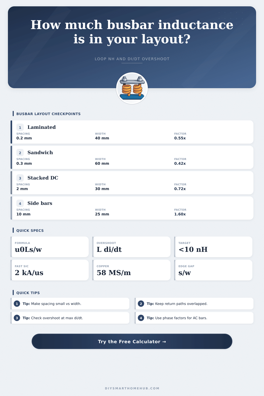
| Laminated positive/negative pair | 0.55x | Wide plates, thin dielectric, high overlap | Strong cancellation, low loop area |
| Sandwich return plane | 0.42x | Current layer between return layers | Very low external field and low stray loop |
| Stacked DC pair | 0.72x | Two bars directly above each other | Good cancellation if terminal exits are short |
| Spaced twin bars | 1.25x | Parallel bars with visible air gap | More loop area and weaker mutual coupling |
| Side-by-side bars | 1.60x | Adjacent bars on same plane | Large loop area unless return path is very close |
| Coaxial or wrapped return | 0.38x | Return surrounding outgoing current | High cancellation, especially for pulse loops |
🔀Phase Arrangement Factors
| Phase arrangement | Factor | Use when | Planning note |
|---|---|---|---|
| DC pair or single commutation loop | 1.00x | Capacitor to half-bridge busbars | Direct outgoing and return current pair |
| Split phase L1/L2/neutral bars | 1.10x | Residential or UPS split bus | Neutral current may not cancel the same loop |
| Three-phase flat A-B-C spacing | 1.18x | Flat phase bars without interleaving | Wider phase spacing raises stray field |
| Three-phase transposed or nested | 0.85x | Compact inverter phase output block | Some magnetic cancellation between nearby phases |
| Six-pulse rectifier bus | 0.95x | Rectifier bridge with DC link nearby | Commutation moves between phase pairs |
| Interleaved phase-return layers | 0.72x | Layered AC/DC busbar assembly | Return paths stay close across the stack |
📐Formula and Geometry Checks
| Check | Screening formula | Good range | Why it matters |
|---|---|---|---|
| Parallel plate inductance | L = u0 x l x s / w | s/w below 0.05 | Valid when plates are wide compared with spacing |
| Voltage overshoot | V = L x di/dt | Below device margin | Fast switches turn a few nH into real voltage |
| Loop energy | E = 0.5 x L x I² | Lower is better | Stored field energy can ring with capacitance |
| Current density | J = Irms / area | 1 to 4 A/mm² | Thermal screening for copper or aluminum bars |
| End allowance | Added from tab length | Keep tabs short | Terminals and bends often dominate compact buses |
🔍Common Busbar Geometry Benchmarks
| Application | Length | Spacing | Width | Typical loop result |
|---|---|---|---|---|
| Low-voltage inverter laminated bus | 0.20 to 0.35 m | 0.3 to 1.0 mm | 35 to 80 mm | 3 to 12 nH |
| SiC module DC link | 0.06 to 0.18 m | 0.15 to 0.6 mm | 40 to 90 mm | 1 to 6 nH |
| EV traction bus stack | 0.30 to 0.70 m | 0.4 to 2.0 mm | 50 to 120 mm | 6 to 25 nH |
| UPS spaced copper link | 0.40 to 1.20 m | 5 to 25 mm | 25 to 80 mm | 40 to 250 nH |
| Panelboard service bars | 0.60 to 1.80 m | 15 to 60 mm | 20 to 60 mm | 100 nH plus |
💡Calculation Tips
In power electronics design circles, there is endless discussion about current carrying capacity and thermal resistance. However, nobody mentions loop inductance, which are the worst thing that happens when a silicon carbide switch shuts down.
Your silicon carbide switch doesn’t give a hoot about how efficienty your heat sink is running. What it does care about is the magnetic energy that gets stored in conductor path between itself and the capacitor. That create voltage overshoot and ringing. These issue stress junction.
Why Loop Inductance Matters for SiC Switches
But what do all these numbers mean? Look beyond simple shape of the copper bars and let the calculator above do math for you. You may see a short-looking loop on your schematic, but each circuit path have some inductance. A few nanohenries can produces hundreds of volts at turn off time in high frequency switching uses.
Your busbar may be nothing more than a piece of metal connecting point A to point B, but it’s a spread-out part with an impedance profile from the electromagnetic field’s perspective. You can’t eliminate inductance completely; that’s never the objective. Rather, you want to minimize the loop area created by the returning current and outgoing current. That’s why material choice doesn’t matter as much than layout does for fast edges.
Imagine two bars placed beside one another on same flat plane. This means the current traveling in both directions runs alongside each other at a distance. This produce a fair amount of magnetic flux, or stored electrical energy, which is ready to discharge as voltage when the current shifts suddenly.
On the other hand, if the positive and negative plates are simply stacked upon each other with a thin layer of dielectric material in between them, their respective fields counteract and effectively becomes superimposed so that they cancel out. The tool takes this into account by calculating layout factors, which lower its estimate of inductance for stacked or sandwiched plates compared to separated twin bars.
Terminal tabs and end connections matter, more than most engineer realize. For instance, you can create an ideal laminated busbar with low inductance along its length. You then mess it all up with big, bulky capacitor terminals on each end or long lead frames. Those leads defeat the close magnetic coupling and introduce additional stray inductance which become the vast majority of the whole loop.
The calculator will allow for this real world less than perfect end connection. It’s a reminder that how you connect things is almost as important than what thing is made out of. Keep the loops small by using short tabs and direct mounting points.
No negotiating here. No negotiating here.
A second common misperception is that a wider path mean less inductance. Yes, the width helps create a parallel plate effect, but distance between the positive path and return path is often the most important factor. You get less benefit from increasing bar width beyond some point depending off the gap (the spacing). Shrinking the gap between your plus/minus conductors causes a linear reduction that dominate this tradeoff.
This explains much of the engineering behind how design works. For example, why would they chooses thinner insulators? They might also choose a material for flexible laminates that bends well and holds a tight fit to minimize dielectric gap.
In conclusion, remember that these are all estimates based off perfect, ideal geometry. Phase interleaving, bolt holes, sensor cutouts etc will cause localized disruptions to the magnetic field distribution in real world. The tool serves to set a benchmark against which you can compare various layout approaches so you know if the strategy you’re using is anywhere near the right order of magnitude.
Staying under ten nanohenries is often the difference between stable operation and catastrophic failure for sensitive SiC modules. The secret is to not think about inductance as something that could of been tacked-on at the end of assembly; instead consider it a fundamental part of design from the start. Minimize loop area, maximize overlap and you’ll make system inherently rugged by construction prior to turning on any switches.