Voltage Divider Calculator
Calculate ideal output, loaded output, ADC loading error, worst-case resistor tolerance range, divider current, and resistor power for low-voltage sensing circuits.
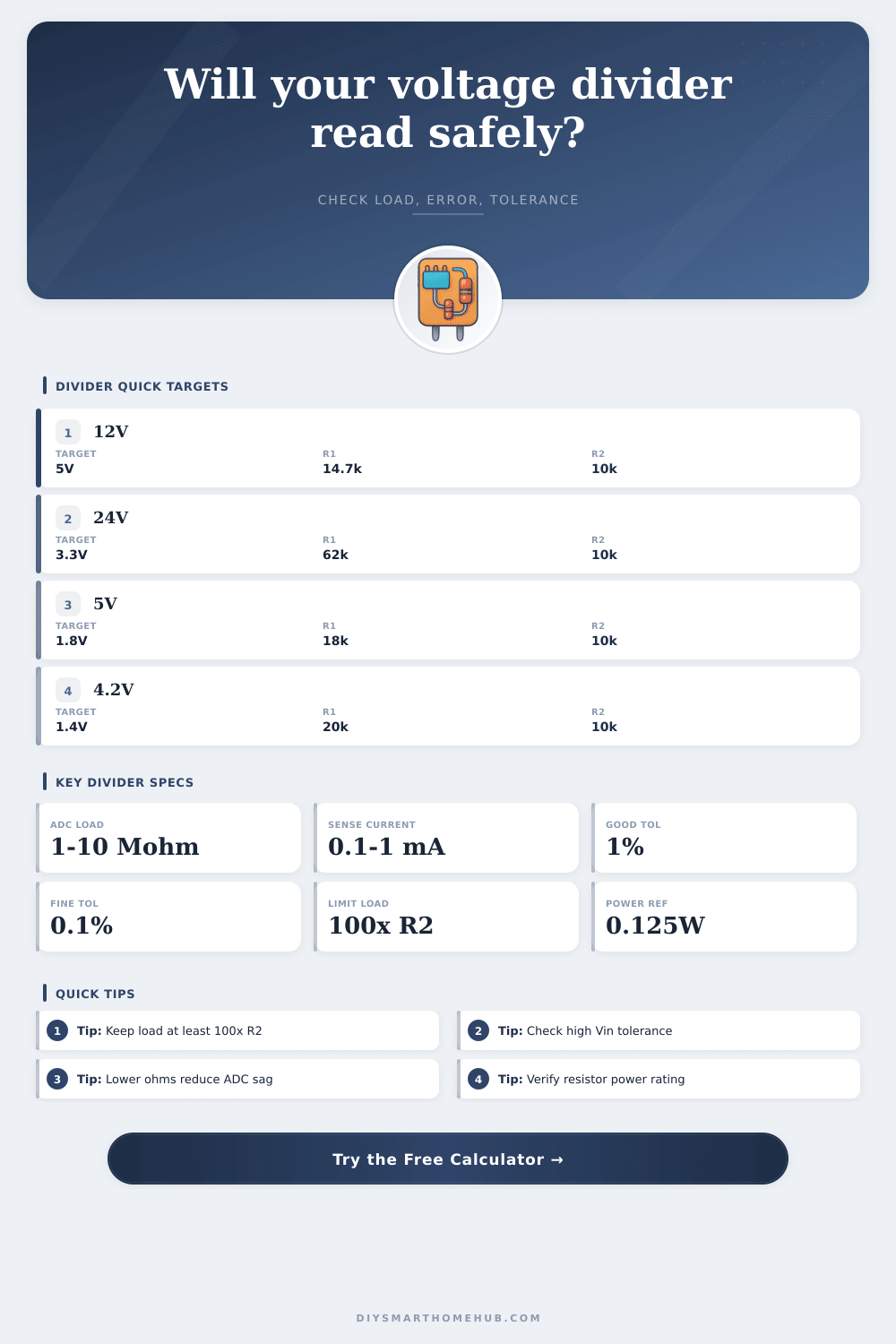
⚡Real divider presets
🔧Divider and load inputs
Formula breakdown
📊Live circuit spec check
🗂Reference tables
| Target circuit | Common input limit | Typical input load | Divider note |
|---|---|---|---|
| Arduino-style 5V ADC | 5.0V max | About 100 Mohm DC, sampling cap dynamic | Keep source impedance under about 10k ohm for fast ADC reads or add a capacitor. |
| ESP32 ADC channel | 3.3V absolute rail limit | High DC load, nonlinear ADC front end | Use margin below 3.3V and calibrate ADC readings in firmware. |
| RP2040 ADC input | 3.3V max | High impedance with sample capacitor | Lower divider resistance improves settling between channel switches. |
| CMOS logic sense pin | Usually VDD plus clamp diode limit | Very high impedance, leakage nA to uA | Divider output must stay below the pin rail at high Vin. |
| Industrial 0-10V ADC module | 3.3V or 5V internal ADC | Often 100k to 1 Mohm front end | External load may already be part of the module input network. |
| Design rule | Formula | Good target | Why it matters |
|---|---|---|---|
| Unloaded output | Vout = Vin x R2 / (R1 + R2) | At least 5% below input limit | Leaves room for supply and resistor tolerance. |
| Loaded R2 | R2eq = R2 || Rload | Rload at least 100 x R2 | Heavy loads pull the output lower than the nominal ratio. |
| Bias current sag | V = (Vin/R1 - Ibias) / conductance | Bias small versus divider current | Very high-value dividers are sensitive to leakage current. |
| Divider current | I = Vin / (R1 + R2) | 0.05 to 1 mA for many sensors | Lower current saves power but increases load and leakage error. |
| Resistor power | P = I squared x R | Use 2x or more margin | Higher Vin and low resistor values can overheat small packages. |
| Vin to target | Example R1 | Example R2 | Ideal output |
|---|---|---|---|
| 12V to 5V | 14.7k ohm | 10k ohm | 4.86V |
| 24V to 3.3V | 62k ohm | 10k ohm | 3.33V |
| 5V to 1.8V | 18k ohm | 10k ohm | 1.79V |
| 4.2V to 1.4V | 20k ohm | 10k ohm | 1.40V |
| 48V to 3.0V | 150k ohm | 10k ohm | 3.00V |
| 10V to 3.3V | 20k ohm | 10k ohm | 3.33V |
| Resistor tolerance | Typical use | Divider impact | Best fit |
|---|---|---|---|
| 5% | General pullups and rough sense lines | Can move ratio several percent | Noncritical threshold detection |
| 1% | Common metal film and SMD values | Good default for ADC scaling | Battery monitors and smart sensors |
| 0.5% | Better matched networks | Improves span accuracy | Repeated sensor boards |
| 0.1% | Precision divider parts | Ratio error is usually below ADC gain error | Reference scaling and calibration fixtures |
🔋Device and spec comparison grid
| Device class | Practical divider current | Input concern | Recommended check |
|---|---|---|---|
| Battery monitor that sleeps | 5 to 50 uA | Quiescent drain | Use higher ohms, then account for ADC acquisition time and leakage. |
| Microcontroller ADC telemetry | 50 to 500 uA | Sample capacitor settling | Keep Thevenin resistance modest or add a small hold capacitor. |
| Logic-level presence detect | 20 to 200 uA | Threshold spread | Compare worst-case low output against VIH and high output against max pin voltage. |
| Industrial analog scaling | 100 uA to 1 mA | Input impedance and noise pickup | Confirm the module load resistance before selecting external values. |
| High-voltage sense front end | 100 uA to 1 mA | Power and voltage rating | Use series parts if a single resistor lacks voltage or power margin. |
💡Divider design tips
A voltage divider circuit are used to take a high voltage and lower it to a lower voltage using two resistor in series. You would use a voltage divider if the voltage from the voltage source that you are measuring is higher than what your chip can accept. This circuit take a measurement from the voltage source at a tap between the two resistors, which provide a lower voltage that your chip can measure.
The voltage divider equation is based off assuming that nothing is connected to the output node of the divider. However, in practice, there will be many component connected to that output node. If a component is connected to the output node, then that component will have some resistance.
Voltage Divider: How It Works and What Can Go Wrong
This resistance will be in parallel with the lower of the two resistors in the divider. Because of this, the output voltage will be lower than that calculated by the voltage divider equation. This error in the output voltage is known as a load error.
The load error will be more pronounced with higher value resistors. For example, if you are using the voltage divider circuit to measure the voltage of a battery, you will likely want to limit the amount of current draw from the battery. However, if the resistance of the analog to digital converter isnt significantly higher than the lower resistor, then the voltage of the battery will be less than the actual voltage of the battery.
Another factor to consider with voltage dividers is the tolerance of the resistors and the variation of the source voltage. Resistors will never have exactly the same value as the one marked on the resistors. Additionally, the voltage of the source can change over time.
If the source voltage is at its maximum, and the top resistor is at its low tolerance limit, and the bottom resistor is at its high tolerance limit, then the circuit could experience an overvoltage fault. In this case, you want to make sure that the output voltage is within a safe level for the device pin. To calculate this, you can calculate the high and low possible output voltage range to ensure it is within the proper range.
Another consideration with voltage dividers is the power dissipation of the resistors. The current flowing through the top resistor will be the highest if the output node is loaded with components. With higher current through the resistor, more power is dissipated as heat.
If the resistor dissipates too much power, it may discolor or fail. Therefore, it is important to calculate the power that each resistor will have to dissipate to make sure it is within the power rating of the resistor. Furthermore, there will often be leakage paths in a real circuit that are not represented in the circuit schematic.
These paths can be caused by moisture on the circuit board or the flux residue left on the board during the circuit board manufacture process. The current through these paths can be significant if the current through the voltage divider is small. This bias current can be modeled with a value in a voltage divider calculator to see if the output voltage will move significant with the addition of this current.
When choosing resistor values, you must balance a few factors. If you choose lower resistor values, the impact of any leakage current will be less, which is helpful if you have a multiplexed analog to digital converter. However, with lower values of resistors, the power draw of the circuit will increase.
If you choose higher resistor values, the circuit will draw less power. However, higher value resistors will be more sensitive to any component connected to the output node. One rule of thumb is to make sure the load resistance is at least one hundred times the value of the lower resistor.
Additionally, the output voltage should be at least five percent below the absolute maximum voltage that is allowed for that pin specification. Finally, another important consideration of voltage dividers is that the output voltage remains within the expected range. You want to make sure that the output voltage is within the expected range despite changes in temperature, supply voltage drift, and resistor tolerance.
To ensure the voltage divider works as expected, calculate the loaded voltage and calculate the worst-case scenario for the voltage divider before you begin laying out your circuit. By calculating these value, you can avoid having to debug the voltage divider once it is built on the circuit board.